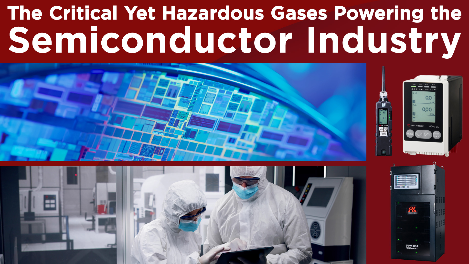
The Critical Yet Hazardous Gases Powering the Semiconductor Industry
Table of Contents
Overview: Semiconductor Manufacturing
Used in everything from smartphones to computers, automobiles, IoT devices and more, semiconductors play a crucial role in digital technology. As digital technology continues to grow, so does semiconductor manufacturing. But with increased semiconductor production comes greater complexity in the manufacturing process, posing additional risks. Semiconductor manufacturing requires the use of chemicals in high-temperature and high-vacuum environments, therefore raising concerns not only about worker safety but also regarding its potential negative impact on the environment.
The semiconductor manufacturing process can be broadly divided into four main stages: design, front-end processing, back-end processing and inspection. The process requires the use of specialized gases, especially during the front-end process, where steps such as wafer surface oxidation, thin film formation, photoresist coating, exposure and development, etching, resist stripping and cleaning occur. The gases used in these processes are rarely found in the natural environment and are manufactured by specialized gas suppliers through sophisticated chemical reactions and specialized manufacturing processes. In this article, we will provide an overview of these gases which play a crucial role in sustaining the core of the semiconductor industry.
Gases Used in Semiconductor Manufacturing
Semiconductor manufacturing requires the use of gases unlike those used in many other industries whose composition and purity must be adapted precisely to their specific purpose of use. In addition to semiconductors, these gases are likewise used in other applications such as the production of optical fiber, solar cells, and fine ceramics. Essential for the production of new materials and developments in technology, these highly specialized gases in turn require highly specialized management.
Here are some examples of gases used in the semiconductor manufacturing processes: Monosilane, disilane, phosphine, arsine, germane, hydrogen selenide, hydrogen fluoride.
Gas-Related Hazards in Semiconductor Manufacturing
Flammability
Corrosiveness
Toxicity
Some gases known as toxic gases are harmful to the human body when inhaled or touched. In order to ensure the safety of workers exposed to these toxic gases, several guidelines and environmental standards have been established. TLV, or Threshold Limit Value, is widely known as an international standard indicating the airborne concentration of hazardous chemical substances. TLV has the following three indicators:
- TLV-TWA (Time-Weighted Average): The concentration averaged over 8 hours a day and 40 hours a week.
- TLV-STEL (Short-Term Exposure Limit): This indicates the 15-minute TWA exposure that should not be exceeded at any time during a workday, even if the 8-hour TWA is within the TLV-TWA.
- TLV-C (Ceiling): The concentration that should not be exceeded during any part of the working exposure.
Many gases used in semiconductor manufacturing including arsine and monosilane are classified as toxic gases, and as such they are subject to extremely low TLV concentration values.
Considering the risks mentioned above, it is imperative that each country establish its own set of guidelines to monitor gas concentration levels and ensure the safety of semiconductor manufacturing as well as industry growth.
Case Studies of Gas Incidents in Semiconductor Facilities
Several serious incidents involving specialty gases have occurred in semiconductor production environments. The following examples illustrate the potential consequences of inadequate gas management.
United States: Arsine Leak at a Semiconductor Facility (1982)
In 1982, a significant arsine gas leak occurred at a gallium arsenide semiconductor production line at a semiconductor facility in New York State. Multiple employees were exposed to the highly toxic gas.
Arsine is known for its severe hematotoxic effects and is considered one of the most hazardous gases used in semiconductor manufacturing. This incident was later documented in investigative reports by U.S. Environmental Protection Agency (EPA) and The National Institute for Occupational Safety and Health (NIOSH), becoming a widely cited example of the dangers associated with toxic gas leaks. It underscored the critical need for highly reliable gas monitoring systems capable of detecting extremely low concentrations.
Japan: Monosilane Explosion at a University Laboratory (1991)
In October 1991, an explosion occurred inside a monosilane cylinder during plasma CVD experimentation at a university laboratory in Japan. Several personnel were affected by the incident.
The root cause was the failure of a deteriorated check valve connected to the cylinder. This malfunction allowed monosilane gas to mix with nitrous oxide inside the container, triggering the explosion.
In addition to the incident, a monosilane leak and explosion accident occurred at a factory in Japan in 1989. In response to this series of accidents, Japan introduced mandatory reporting requirements for certain high-pressure specialty gases and strengthened regulations governing safety equipment such as gas cabinets, alarm systems, emergency shutoff devices, gas abatement systems, backup power supplies, and leak testing instruments. The case highlighted the importance of gas detection and flow monitoring systems that can identify abnormal conditions before they escalate.
South Korea: Hydrogen Fluoride Leak at a Semiconductor Plant (2013)
In January 2013, a hydrogen fluoride gas leak occurred during maintenance work at a semiconductor fabrication facility in Gyeonggi Province. Several workers were affected by the incident.
Hydrogen fluoride is highly corrosive, and the accident received widespread international media coverage. It emphasized the importance of rigorous toxic gas management practices across entire production facilities. The incident also demonstrated the need for robust maintenance procedures for aging equipment and for rapid detection and alarm systems capable of responding immediately to abnormal events.
Challenges in Gas Detection at Semiconductor Plants
Gas detection systems are essential for preventing incidents such as those described above. However, semiconductor manufacturing environments present unique operational challenges.
-
Continuous operation requirements
Semiconductor fabrication facilities typically operate 24 hours a day. A failure in gas detection equipment may necessitate a production shutdown for safety reasons, resulting in significant financial losses. Detection systems with built-in redundancy are therefore required to maintain continuous monitoring even during component failures.
-
Large number of monitoring points and maintenance burden
Cleanroom piping networks and gas cabinets create numerous gas monitoring points throughout the facility. Installing individual detectors at each location increases equipment costs and expands the installation footprint, creating space constraints. In addition, maintenance tasks such as sensor replacement and calibration become increasingly burdensome, and can only be handled by a limited number of personnel.
-
Need for remote status monitoring
It is inefficient to check the status of detectors dispersed throughout a large factory by visiting each location. Therefore, a remote monitoring system is required to centrally manage operational status and alarms via a network. In addition, since gases are not visible, it is difficult to determine from detector data alone whether an actual gas leak has occurred or if it is merely a false alarm. Therefore, even in remote monitoring, a system that enables verification of actual gas leaks is required.
Solutions for Gas Detection Challenges in Semiconductor Facilities
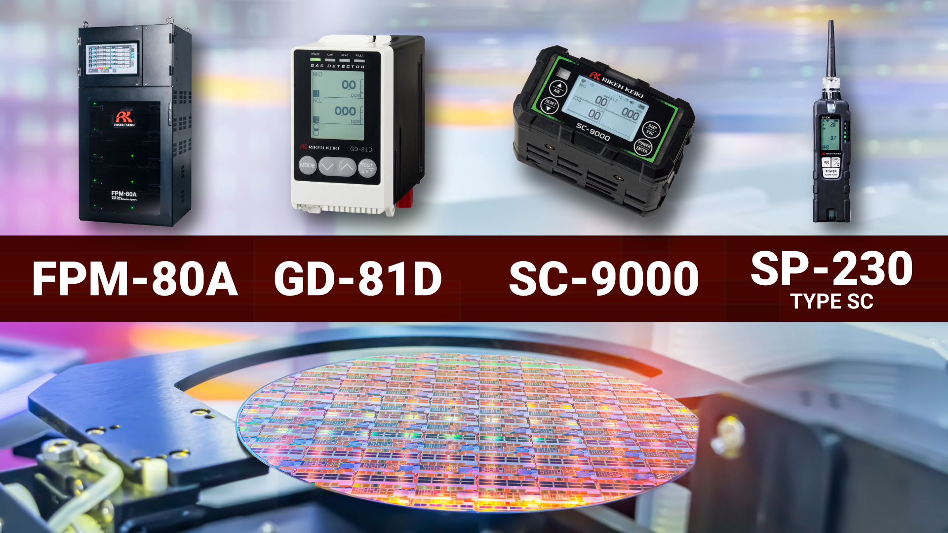
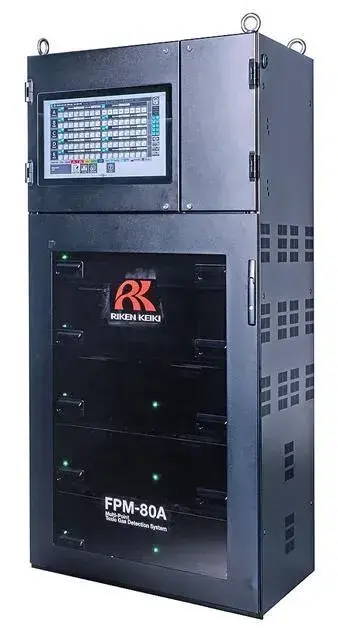
Multi-Point Gas Detection System FPM-80A
This centralized system can monitor up to 80 sampling points simultaneously, enabling the consolidation of multiple detection points and helping reduce the overall installation footprint. Redundant design features for the pump, power supply, and solid-state drive enable automatic switchover to backup components in the event of failure, ensuring uninterrupted detection.
The cassette-type detection tape can be replaced with one hand, and RFID-based tracking enables efficient tape usage management. The system supports multiple communication protocols, including Modbus, Ethernet, and PROFIBUS. A built-in discoloration monitoring camera allows remote visual confirmation of abnormal conditions.
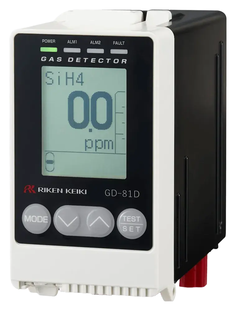
Fixed Gas Detector Head GD-81D
Portable Multi Toxic Gas Detector SC-9000
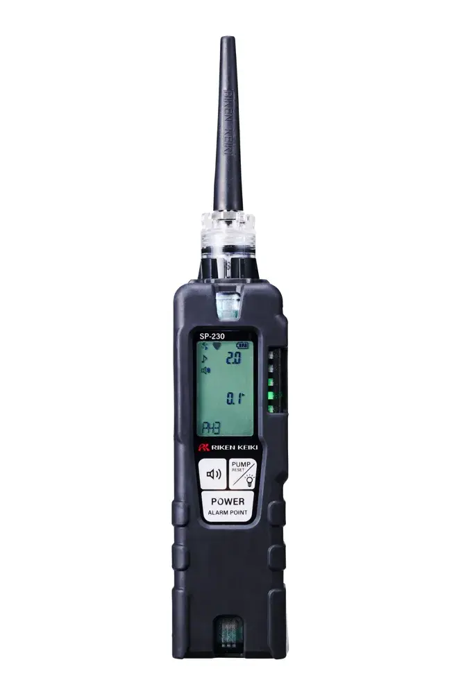
Portable Gas Leak Checker SP-230 TYPE SC (for semiconductor material gas)
PRODUCTS
Product type |
Fixed Gas Detector |
|---|---|
Applications |
|
single/multi |
Multi |
Product type |
Fixed Gas Detector |
|---|---|
Applications |
|
single/multi |
Single, Multi |

Product type |
Portable Gas Detector |
|---|---|
Applications |
|
single/multi |
Multi |
Product type |
Portable Gas Detector |
|---|---|
Applications |
|
single/multi |
Multi |
Want to hear from an expert?
You may also be
interested in
Protecting Product Quality with Automated Air Intake Control
Outside air brought in through the plant’s air intake system can cause product quality issues. This article explains outside-air-related risks and introduces an approach using tape-type gas detection for high-sensitivity detection and automated control.
Why Redundancy is the Lifeline of Semiconductor Manufacturing? The “Dual-Backup” That Prevents Production Stop During Equipment Failures.
Discover how redundancy in semiconductor manufacturing, particularly through the FPM-80A gas detector, ensures continuous operation and mitigates costly production stops.
The Evolution of Gas Detection Tape: 180 Days of Maintenance-Free Operation
Discover how the FPM-80A gas detection tape offers 180 days of maintenance-free operation, enhancing safety and reducing costs in semiconductor manufacturing.
Publications