Skip to content

Table of Contents

    What Are Organic Semiconductors? How Are Inorganic Semiconductors Different?

    Organic semiconductors are increasingly being used as core materials in technologies such as OLED displays, perovskite solar cells, and wearable sensors. 
     
    Although the term "organic semiconductor" is becoming more familiar, the differences between organic semiconductors and conventional inorganic semiconductors such as silicon, as well as the reasons behind their expanding range of applications, are not always clearly understood. 
     
    This article explains the key characteristics of organic semiconductors, how they differ from inorganic semiconductors, and where they are currently being applied. It also introduces the concept of energy levels, a critical factor in the performance of organic electronic devices. 

    Organic vs. Inorganic Semiconductors

    Organic semiconductors are organic materials that exhibit semiconductor properties. Compared with inorganic semiconductors based on crystalline materials such as silicon, they differ significantly in structure, manufacturing processes, and performance characteristics.

    Organic vs. Inorganic Semiconductors

      Organic Semiconductors Inorganic Semiconductors
    Structure Carbon-based molecules Crystalline materials such as silicon
    Characteristics Flexible and lightweight Rigid and relatively heavy
    Manufacturing Process Coating and printing processes High-temperature deposition and lithography
    Design Flexibility Properties can be tuned through molecular design Performance largely determined by crystal structure and material properties
    Typical Applications Flexible and thin-film devices High-speed processing, high durability, and highly integrated circuits

    The strong crystalline structure of inorganic semiconductors makes them suitable for applications requiring high-speed operation and long-term durability. In contrast, organic semiconductors rely on relatively weak intermolecular interactions, making them well suited for thin, lightweight, and flexible electronic devices.

    Another important difference lies in manufacturing. Inorganic semiconductors typically require high-temperature and vacuum-based deposition processes followed by fine patterning techniques. Organic semiconductors, on the other hand, can often be fabricated as thin films using low-temperature coating or printing processes. As a result, they have the potential to reduce manufacturing costs compared with conventional semiconductor technologies.


    Key Applications of Organic Semiconductors

    Because of their flexibility and lightweight nature, organic semiconductors enable applications that differ from those of traditional inorganic semiconductors. Several representative examples are outlined below.

    OLEDs

    Organic Light Emitting Diodes (OLEDs) are widely used in smartphones, televisions, and automotive displays.

    By utilizing the light-emitting properties of organic materials, OLEDs deliver high contrast ratios and vivid color reproduction. Unlike liquid crystal displays (LCDs), which require a backlight, OLED pixels emit light directly. This enables thinner displays, curved form factors, and innovative designs such as foldable displays.

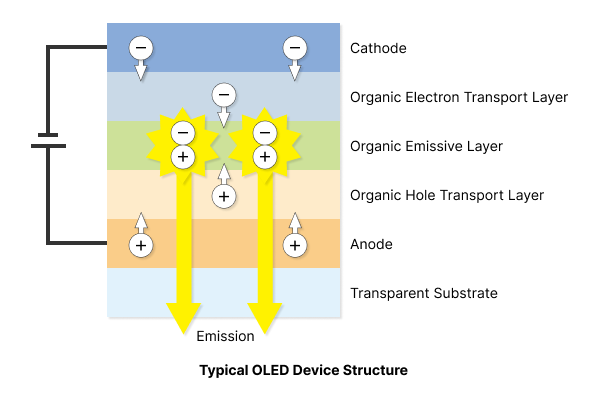
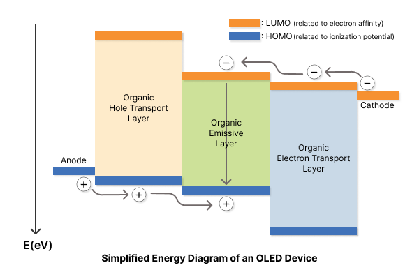
    OLED devices consist of multiple stacked organic material layers, and the properties of each layer directly affect overall device performance. In particular, if the energy levels between adjacent materials are not properly aligned, charge transport can be hindered, reducing luminous efficiency and device lifetime.

    Typical OLED Device Structure

    Perovskite Solar Cells

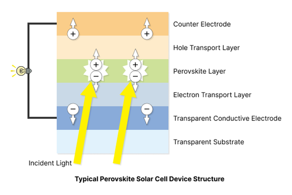
    Perovskite solar cells utilize materials with a crystal structure known as the perovskite structure. Their lightweight nature, ease of film formation, and high light absorption efficiency have driven rapid research and development in recent years.

    One of their major advantages over conventional silicon solar cells is that they can be fabricated as thin-film devices. Because the perovskite layer functions as an extremely thin light-absorbing layer, lightweight and flexible solar cells can be produced. This opens possibilities for installations in locations where traditional solar panels are difficult to deploy.

    perovskite_600x400-1
    Several perovskite solar cell configurations are currently under development:

    • Film-Type Perovskite Solar Cells
      Formed on flexible film substrates, these devices offer low weight and flexibility. Potential applications include building facades and curved surfaces where conventional solar panels are impractical.

    • Glass-Type Perovskite Solar Cells
      Using glass substrates, these devices can potentially serve as both power-generating solar cells and architectural glass materials for windows and building exteriors. Glass substrates also provide excellent thermal and chemical stability, making them suitable for device evaluation and long-term durability studies.

    In addition to single-junction perovskite cells, tandem solar cells that combine perovskite and silicon layers are also being actively researched. In tandem structures, each layer absorbs different wavelengths of light, enabling higher conversion efficiencies than either technology alone.

    Despite these advantages, several challenges remain before widespread commercialization can be achieved. Material stability and interface engineering are particularly important. If energy levels between adjacent materials are not properly matched, charge transport can be impeded, reducing both power conversion efficiency and device lifetime.

    Organic Thin-Film Transistors (OTFTs)

    Organic Thin-Film Transistors (OTFTs) utilize organic semiconductor materials and are attracting attention for flexible and lightweight electronic applications.

    Because organic semiconductors can be processed at relatively low temperatures, they can be fabricated directly on plastic substrates with limited heat resistance.

    These characteristics have led to extensive research into bendable electronics and large-area electronic circuits. Potential applications include display control circuits for electronic paper, wearable devices, smart labels, and other thin, flexible electronic products.

    OTFTs are also being explored for sensor arrays and simple electronic circuits that can be manufactured over large surface areas. This makes them promising for applications such as smart packaging and intelligent building materials that incorporate electronic functionality directly into conventional products.

    As with other organic semiconductor devices, OTFT performance is highly dependent on the interface between the organic semiconductor material and the electrode. Improper alignment of energy levels between materials can hinder charge transport and negatively affect transistor performance.


    Why Energy Levels Matter in Organic Devices

    As organic semiconductor applications continue to expand, the relationship between material energy levels and electrodes[RM1.1][圭立1.2] has become a critical factor influencing device performance.

    Although organic semiconductors can be manufactured using coating and printing techniques, material characteristics may vary due to film formation conditions or differences between production lots. Consequently, understanding material energy levels is important not only during research and development but also throughout manufacturing and quality control processes.

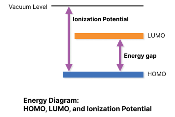
    One important parameter is the ionization potential, which indicates how easily electrons can be removed from a material. Ionization potential corresponds to the energy of the Highest Occupied Molecular Orbital (HOMO).

    Since hole transport occurs through the HOMO level, this energy is a key indicator when evaluating hole injection characteristics at material interfaces.

    Similarly, electron affinity is an important parameter related to electron injection performance. Electron affinity corresponds to the energy level of the Lowest Unoccupied Molecular Orbital (LUMO).

    The energy difference between the HOMO and LUMO levels, known as the HOMO-LUMO gap, can be determined from optical absorption measurements using a UV-Visible spectrophotometer. By combining ionization potential measurements with the HOMO-LUMO gap, the LUMO energy level can be calculated.

    These energy-level parameters provide valuable insight into the electronic behavior of organic semiconductor materials.
    OLEDenelgy-1
    energy_diagram_600x400

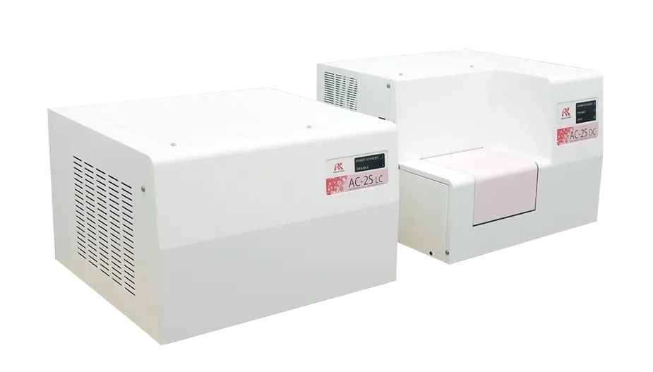
    To support rapid evaluation of these properties, RIKEN KEIKI offers the AC Series.
    Visit the AC Series product page.


    Measuring Ionization Potential with the AC Series

    The AC Series is a photoelectron yield spectroscopy in air (PYSA) system,  based on open-counter technology invented by Dr. Masayuki Uda during his time at RIKEN.

    Many conventional ionization potential measurement systems require vacuum environments and often take several hours to complete a measurement. In contrast, the AC Series does not require a vacuum environment and can measure ionization potential in air in about 5 minutes.

    This capability enables rapid screening of candidate materials during research and development. It also supports quality control in manufacturing environments by evaluating lot-to-lot variations and material degradation during storage.

    As a result, the AC Series provides a versatile measurement solution for organic semiconductor materials, from research through mass production.

    See a comparison of the AC Series with other ionization potential measurement methods.

    Conclusion

    Organic semiconductors differ significantly from inorganic semiconductors in both structure and manufacturing processes, enabling a growing range of applications including OLEDs and perovskite solar cells.

    In organic electronic devices, material energy levels play a critical role in determining device performance. One of the most important parameters related to these energy levels is ionization potential.

    Efficient evaluation of ionization potential can be achieved using dedicated measurement instruments such as the AC Series, supporting both materials development and production quality control for next-generation organic semiconductor technologies.

    PRODUCTS

    Ionization Potential & Work Function Analyzer
    AC Series

    Product type

    Surface Analyzer

    Applications

    single/multi

    ← →
    inquire_slash

    Want to hear from an expert?

    Our team will be happy to help. Let’s find the right solution for you.

    Publications

    case_img-1
    See how companies across different industries are using our advanced gas detectors to prevent accidents, ensure compliance, and enhance safety. Exclusive case studies inside!

    case_img-1